Method of forming lattice matched layer over a surface of a silicon substrate
Abstract
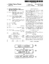
A method of forming lattice matched single crystal wide bandgap II-VI compound semiconductor films over a silicon substrate includes first cleaning (10) the silicon substrate. A passivation layer is formed (18), which may comprise arsenic, germanium, or CaF2, among others. The lattice matched layer is then grown (26) on the passivation layer.
Collections
Citation
(2002). Method of forming lattice matched layer over a surface of a silicon substrate. United States. Patent and Trademark Office; Texas A&M University. Libraries. Available electronically from https : / /hdl .handle .net /1969 .1 /176696.