| dc.creator | Kirk, Wiley P. | |
| dc.creator | Zhou X, Joe | |
| dc.creator | Gnade, Bruce E. | |
| dc.creator | Cho, Chih-chen | |
| dc.date.accessioned | 2019-06-17T16:56:48Z | |
| dc.date.available | 2019-06-17T16:56:48Z | |
| dc.date.issued | 2002-07-16 | |
| dc.identifier.uri | https://hdl.handle.net/1969.1/176696 | |
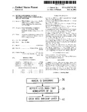
| dc.description.abstract | A method of forming lattice matched single crystal wide bandgap II-VI compound semiconductor films over a silicon substrate includes first cleaning (10) the silicon substrate. A passivation layer is formed (18), which may comprise arsenic, germanium, or CaF2, among others. The lattice matched layer is then grown (26) on the passivation layer. | en |
| dc.language | eng | |
| dc.publisher | United States. Patent and Trademark Office | |
| dc.rights | Public Domain (No copyright - United States) | en |
| dc.rights.uri | http://rightsstatements.org/vocab/NoC-US/1.0/ | |
| dc.title | Method of forming lattice matched layer over a surface of a silicon substrate | en |
| dc.type | Utility patent | en |
| dc.format.digitalOrigin | reformatted digital | en |
| dc.description.country | US | |
| dc.contributor.assignee | Texas Instruments Incorporated | |
| dc.contributor.assignee | Texas A&M University System | |
| dc.identifier.patentapplicationnumber | 08/340097 | |
| dc.subject.uspcprimary | 117/84 | |
| dc.subject.uspcother | 117/90 | |
| dc.subject.uspcother | 438/761 | |
| dc.subject.uspcother | 438/763 | |
| dc.date.filed | 1994-11-15 | |
| dc.publisher.digital | Texas A&M University. Libraries | |
| dc.subject.cpcprimary | C30B 29/48 | |
| dc.subject.cpcprimary | C30B 23/02 | |