| dc.creator | Pandey, Raghvendra K. | |
| dc.creator | Raina, Kanwal K. | |
| dc.creator | Solayappan, Narayanan | |
| dc.date.accessioned | 2019-06-17T16:55:39Z | |
| dc.date.available | 2019-06-17T16:55:39Z | |
| dc.date.issued | 2000-11-28 | |
| dc.identifier.uri | https://hdl.handle.net/1969.1/176650 | |
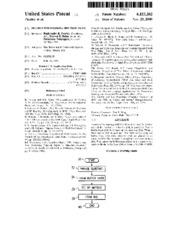
| dc.description.abstract | A method for forming SbSI thin films is formed. In the first step of the method, a substrate (14) is provided. Next a buffer layer (16) is formed on the substrate (14). Then, a SbSI source (12) is provided. The SbSI source (12) and buffer layer (16) with substrate (14) are placed in an ampoule (10). The ampoule is heated in a two-zone furnace (11). This causes the SbSI source (12) to form a vapor which reacts with the buffer layer (14) to form a thin film of SbSI. | en |
| dc.language | eng | |
| dc.publisher | United States. Patent and Trademark Office | |
| dc.rights | Public Domain (No copyright - United States) | en |
| dc.rights.uri | http://rightsstatements.org/vocab/NoC-US/1.0/ | |
| dc.title | Method for forming SbSI thin films | en |
| dc.type | Utility patent | en |
| dc.format.digitalOrigin | reformatted digital | en |
| dc.description.country | US | |
| dc.contributor.assignee | The Texas A&M University System | |
| dc.identifier.patentapplicationnumber | 09/252121 | |
| dc.subject.uspcprimary | 427/255.4 | |
| dc.subject.uspcother | 427/248.1 | |
| dc.subject.uspcother | 427/372.2 | |
| dc.date.filed | 1999-02-18 | |
| dc.publisher.digital | Texas A&M University. Libraries | |
| dc.subject.cpcprimary | C23C 14/024 | |
| dc.subject.cpcprimary | C23C 14/06 | |