| dc.creator | Murphy, Oliver J. | |
| dc.creator | Bockris, John O. | |
| dc.date.accessioned | 2019-06-17T16:59:27Z | |
| dc.date.available | 2019-06-17T16:59:27Z | |
| dc.date.issued | 1988-02-02 | |
| dc.identifier.uri | https://hdl.handle.net/1969.1/176786 | |
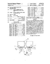
| dc.description.abstract | A photo-activated semiconductor device is adapted to be exposed to light energy. Two physically separated electrocatalysts are placed in electrical contact with the photo-activated semiconductor device. An electrolytic solution physically separated from the semiconductor device is placed in electrical contact with both electrocatalysts. A method for supplying electrical energy to an anode and a cathode is an electrochemical reaction zone containing an electrolytic solution which comprises positioning a photo-activated semiconductor device having separate donor and acceptor regions external to an electrolytic solution. The donor region is electrically connected to a cathode and the acceptor region is electrically connected to the anode. A portion of the photo-activated semiconductor device is exposed to a source of radiation which is external to the reaction zone. The products derived from the electrolytic solution are collected for later use. | en |
| dc.language | eng | |
| dc.publisher | United States. Patent and Trademark Office | |
| dc.rights | Public Domain (No copyright - United States) | en |
| dc.rights.uri | http://rightsstatements.org/vocab/NoC-US/1.0/ | |
| dc.title | One-unit photo-activated electrolyzer | en |
| dc.type | Utility patent | en |
| dc.format.digitalOrigin | reformatted digital | en |
| dc.description.country | US | |
| dc.contributor.assignee | The Texas A&M University System | |
| dc.identifier.patentapplicationnumber | 06/589427 | |
| dc.subject.uspcprimary | 204/242 | |
| dc.subject.uspcother | 136/244 | |
| dc.subject.uspcother | 429/111 | |
| dc.date.filed | 1984-03-14 | |
| dc.publisher.digital | Texas A&M University. Libraries | |
| dc.subject.cpcprimary | C25B 1/55 | |