Gate adjusted resonant tunnel diode device and method of manufacture
Abstract
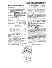
A gated resonant tunneling diode has a semiconductor mesa formed on a semiconductor substrate, a tunneling barrier layer between the mesa and the substrate, and a gate layered over the substrate about the mesa and aligned in close proximity to the tunneling barrier layer. A control voltage on the gate laterally constricts a potential well in the tunneling barrier to control the electrical size of a channel within which tunnelling occurs across the tunneling barrier layer. Preferably the gate and the tunneling layer are disposed at the base of the mesa, and the gate makes a rectifying Schottky junction in connection with the tunneling barrier layer. The device is constructed using an anisotropic etch to form the mesa with an undercut wall and a top portion overhanging the undercut wall, and a nonconformal deposition of gate material to align the gate with the top portion of the mesa.
Collections
Citation
(1992). Gate adjusted resonant tunnel diode device and method of manufacture. United States. Patent and Trademark Office; Texas A&M University. Libraries. Available electronically from https : / /hdl .handle .net /1969 .1 /177230.