Jitter cancellation method for continuous-time sigma-delta modulators
Abstract
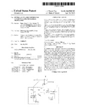
A continuous-time delta-sigma analog-to-digital converter (ADC) is disclosed. The ADC includes a loop filter, a loop quantizer, and a clock-jitter tolerant digital-to-analog converter (DAC). The clock-jitter tolerant DAC includes a dual switched-current (SI) DAC, a switched-capacitor (SC) DAC, an adder, and a switched-capacitor-resistor (SCR) injection circuit. The dual SI DAC provides two identical analog signals from the feedback digital signal of a loop quantizer within the ADC. The SC DAC provides an error-free reference signal from the feedback digital signal. The adder subtracts one of the two analog signals from the error-free reference signal to obtain an inverted jitter-induced error signal. The SCR injection circuit then injects the inverted jitter-induced error signal, delayed by one clock-cycle, in the form of a half-delay return-to-zero exponentially decaying waveform into the loop filter.
Collections
Citation
(2012). Jitter cancellation method for continuous-time sigma-delta modulators. United States. Patent and Trademark Office; Texas A&M University. Libraries. Available electronically from https : / /hdl .handle .net /1969 .1 /176987.