Method of forming a conductive pattern by removing a compound with heat in a substantially inert atmosphere
Abstract
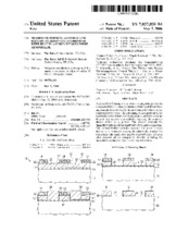
A method for forming a conductive or magnetic pattern for a semiconductor or other electronic device includes patterning a mask layer outwardly from a conductive layer of the semiconductor device. The patterning defines portions of the conductive layer where vias through the conductive layer are desired. The method also includes exposing the semiconductor device to a plasma. The plasma converts the unmasked portions of the conductive layer into a compound. The method further includes exposing the semiconductor device to a treatment process to selectively remove the compound. The mask layer may be removed either before or after removal of the compound, thereby providing the unmasked conductive layer in the desired pattern.
Subject
438/669257/E21.3
257/E21.309
257/E21.311
257/E21.592
438/706
H01L 21/321
H01L 21/32134
H01L 21/32136
H01L 21/76888
Collections
Citation
(2006). Method of forming a conductive pattern by removing a compound with heat in a substantially inert atmosphere. United States. Patent and Trademark Office; Texas A&M University. Libraries. Available electronically from https : / /hdl .handle .net /1969 .1 /176816.